views
Washington: Researchers have developed a new device that could significantly boost the quality of images on smartphones, computer displays, TVs and inkjet printers.
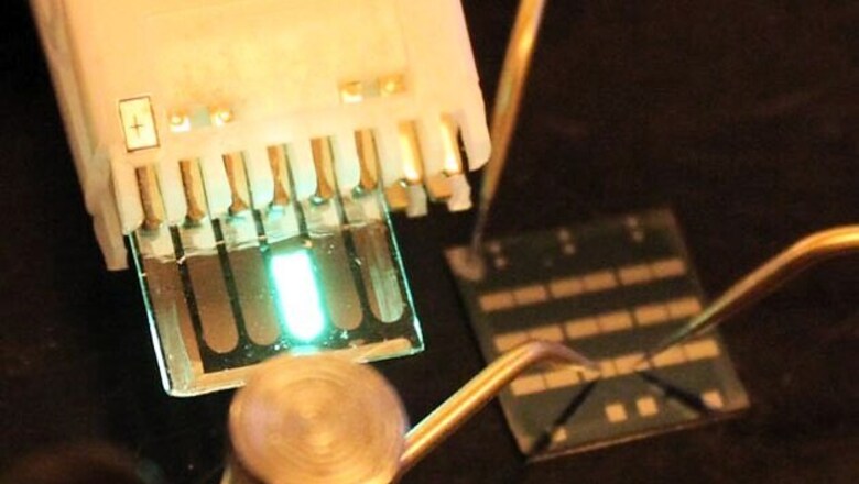
Researchers from the University of California, Los Angeles have developed inexpensive, high-mobility semiconductors for liquid crystal displays (LCD) and organic light-emitting diode (OLED) displays.
"Our semiconductor process is faster, less expensive and more reliable than existing processes," said Yang Yang, the Carol and Lawrence E Tannas Jr Professor of Engineering at the UCLA Henry Samueli School of Engineering and Applied Science.
"We strongly believe it can be used as a technology to replace existing processes and scale up production of thin-film transistors," Yang said.
LCDs and OLEDs use millions of pixels to form text and images on the screen. Thin-film transistors, or TFTs, are the key component of the technology that controls the brightness and colour provided by each pixel.
Typically, a transistor's performance is judged by electron "mobility", or the ability to precisely adjust the voltage and current that turn pixels on and off.
Transistors with higher electron mobility adjust the screen's colour and brightness more easily and with greater energy efficiency than low-mobility devices.
Currently, amorphous silicon-based TFTs are the most popular technology in LCDs, but they suffer low mobility. This is why, when watching a baseball game on a large LCD TV, viewers can often see the "trail" of the ball when it's thrown or hit.
The UCLA-developed product, a non-silicon based amorphous oxide semiconductor TFT, offers mobility that is 10 to 20 times greater than that of an amorphous silicon-based TFT.
The device, which is composed of indium gallium zinc oxide and indium tin zinc oxide, has channels that are designed differently than those in other TFTs.
Currently, amorphous oxide semiconductor TFTs are prepared by a process that requires a large vacuum chamber and a costly coating procedure.
UCLA researchers used a solution process, akin to applying a coat of paint to an object and then baking it in an oven.
"The improved mobility represents a breakthrough for solution-processed metal oxide TFTs," said You Seung Rim, a postdoctoral researcher in UCLA's materials science and engineering department and the lead author of the research.
"Our device's performance is comparable to that of commercial TFTs, but it can be produced at a much lower cost," Rim said.
The research was published in the journal Advanced Materials.


Comments
0 comment